
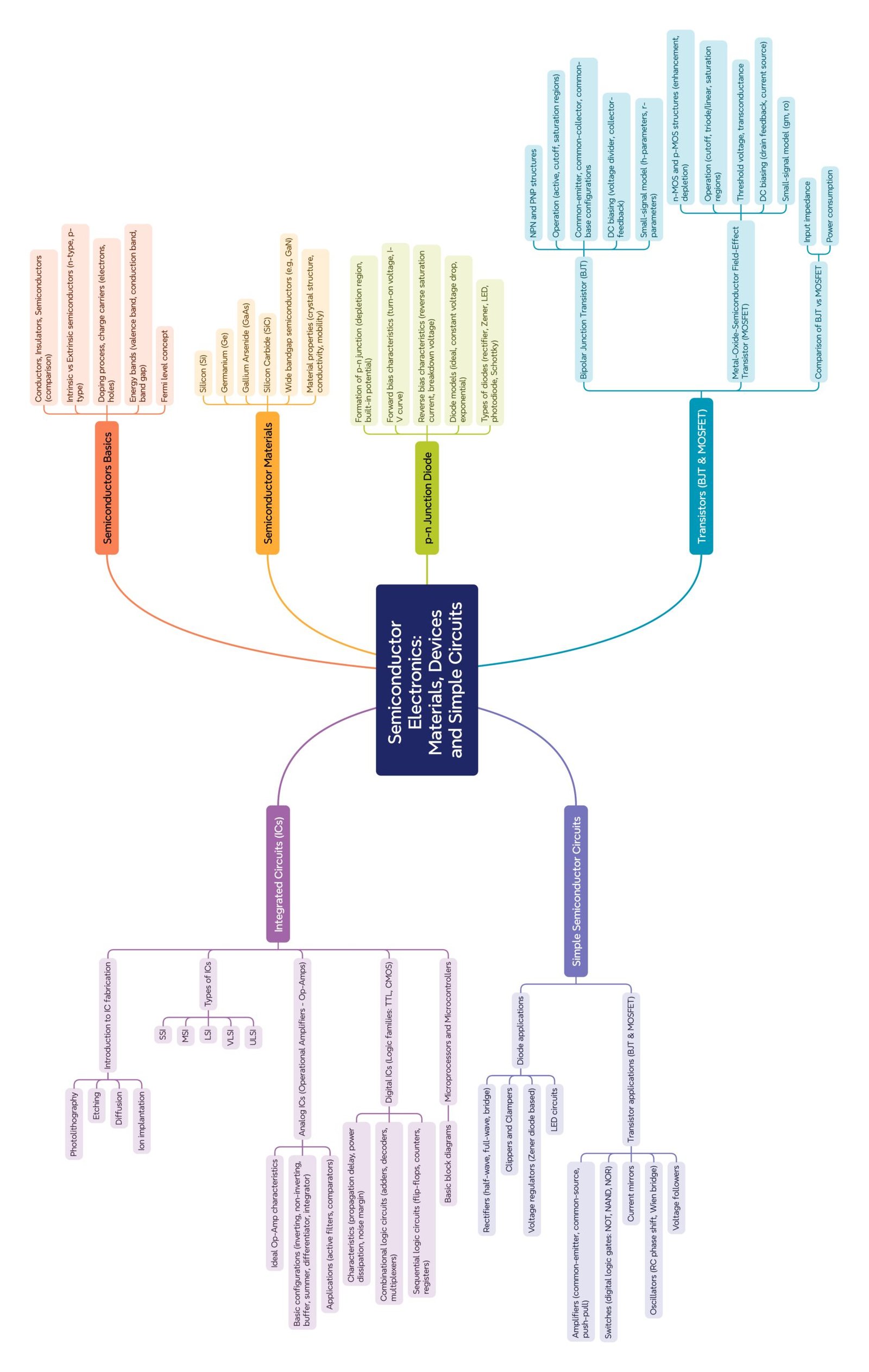
Class 12 : Physics (English) – Chapter 14: Semiconductor Electronics: Materials, Devices and Simple Circuits
EXPLANATION & SUMMARY
🌿 Introduction
The field of semiconductor electronics has revolutionized modern life. Every computer, smartphone, satellite, and medical imaging device depends on semiconductors. Their uniqueness lies in controllable conductivity — they can behave like insulators or conductors depending on temperature, light, electric fields, or impurity doping.
In this chapter, we study:
🔵 Classification of materials and energy bands
🟢 Intrinsic vs extrinsic semiconductors
🔴 p–n junction and its properties
🟡 Devices like diodes, rectifiers, Zener diodes, BJTs, and logic gates
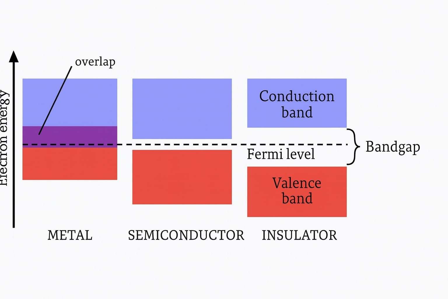
⚡ Classification of Materials
Conductors
➡️ Examples: Copper, Aluminum.
➡️ Band gap ≈ 0 eV.
➡️ High density of free electrons, conduction occurs easily.
Insulators
➡️ Examples: Wood, Glass, Plastic.
➡️ Band gap > 5 eV.
➡️ No conduction under normal conditions.
Semiconductors
➡️ Examples: Silicon (Eg ≈ 1.1 eV), Germanium (Eg ≈ 0.7 eV).
➡️ Moderate conductivity.
➡️ Conductivity increases with temperature (opposite to metals).
➡️ Conductivity can be engineered by doping.
✏️ Note: Semiconductors are the “engineered materials” that enabled the electronics age.
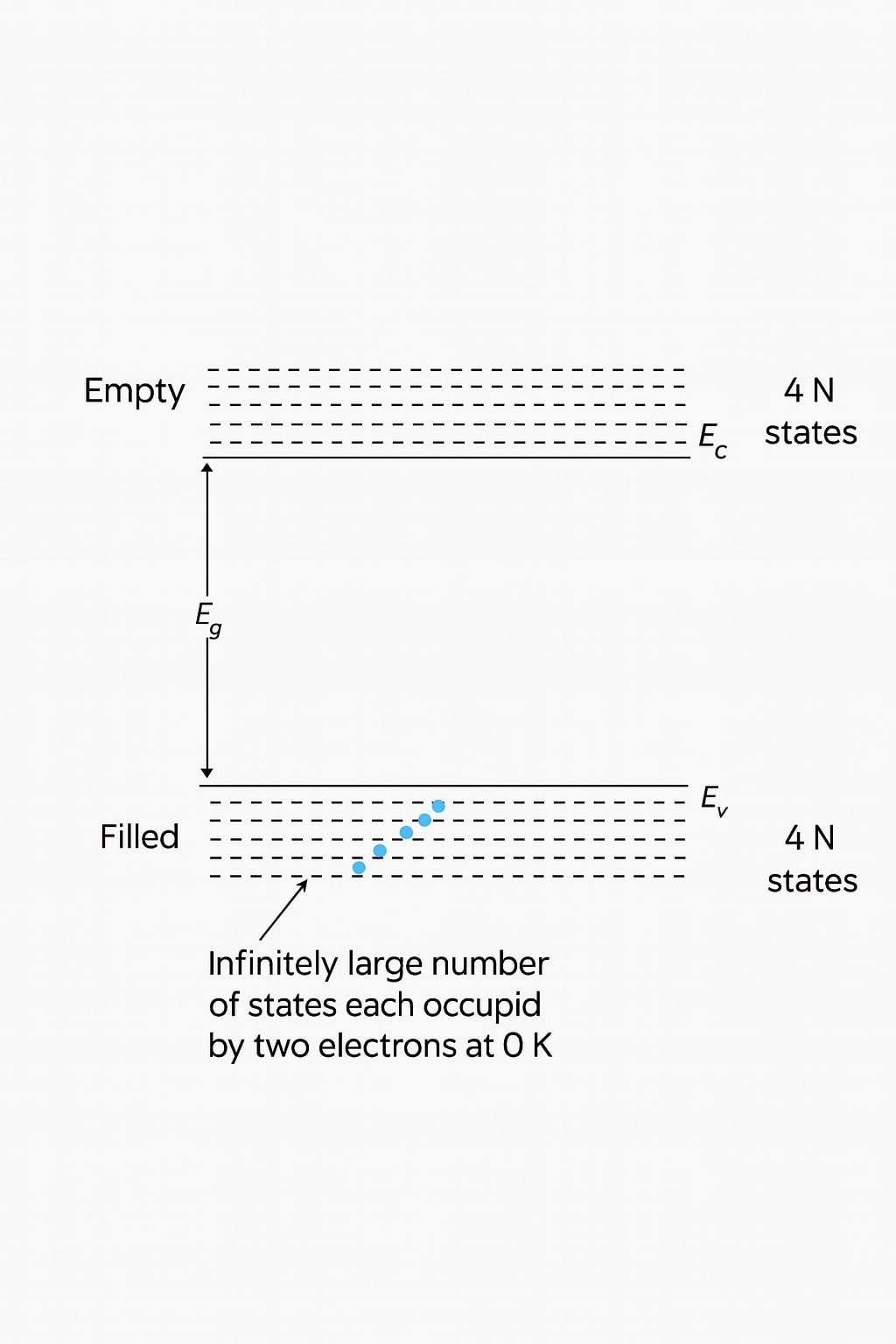
🧠 Energy Band Theory
💡 Concept: In a crystal, discrete energy levels form bands.
Valence Band: Highest occupied band.
Conduction Band: Free electrons move here.
Band Gap (Eg): Separation between conduction and valence band.
✔️ Metals: Eg ≈ 0 (overlap).
✔️ Insulators: Eg > 5 eV.
✔️ Semiconductors: Eg ≈ 1 eV.
At room temperature, some electrons gain energy to jump to conduction band, leaving behind holes. Both contribute to current.
🔬 Intrinsic & Extrinsic Semiconductors
Intrinsic Semiconductor
➡️ Pure Si or Ge.
➡️ Conduction only by thermally generated electron-hole pairs.
➡️ Limited conductivity.
Extrinsic Semiconductor
➡️ Doped with impurities to enhance conductivity.
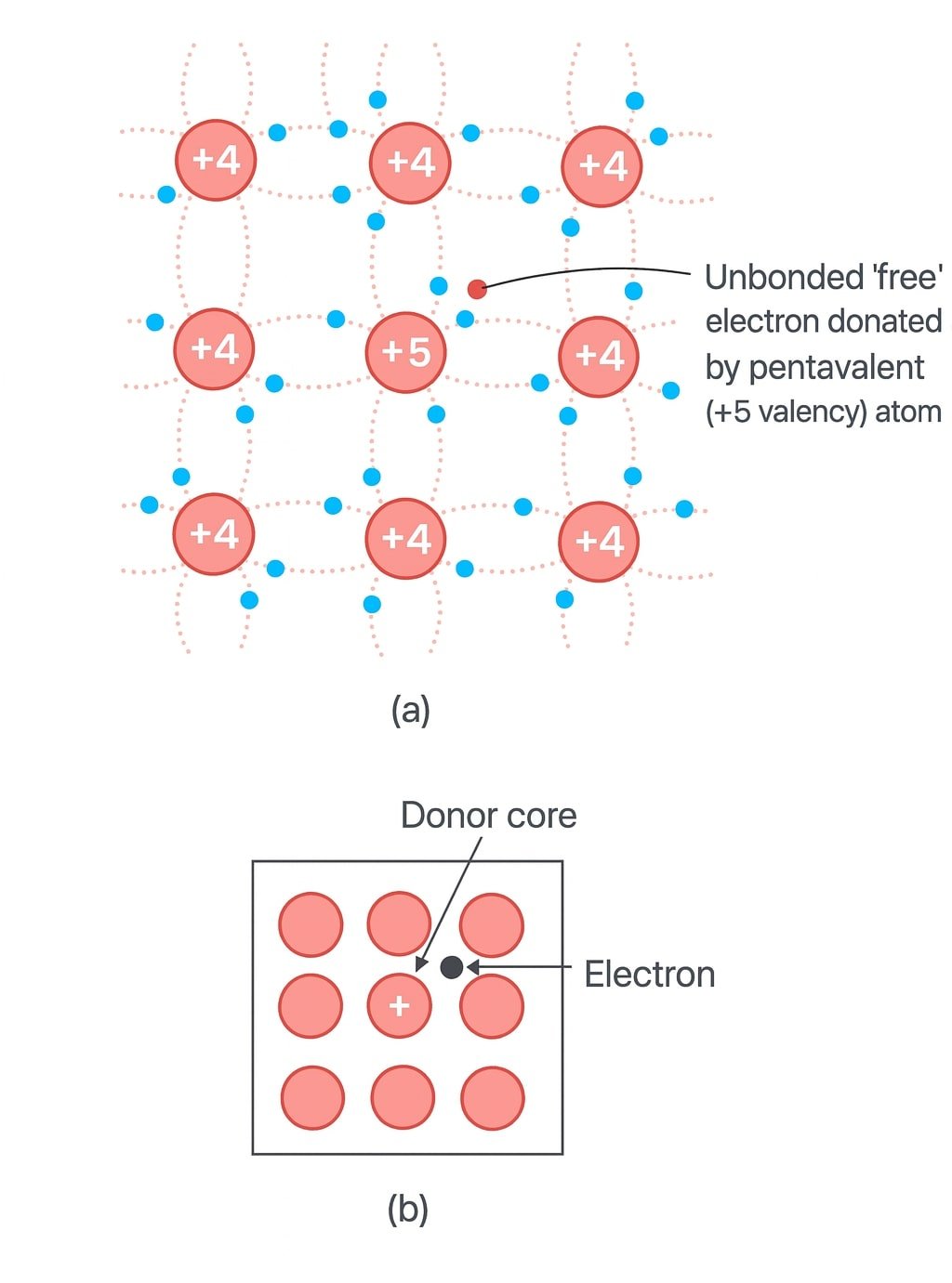
n-type: Pentavalent dopant (P, As, Sb). Extra electrons → majority carriers.
p-type: Trivalent dopant (B, Al, In). Extra holes → majority carriers.
✔️ Charge neutrality remains intact — the crystal stays electrically neutral.
🌐 The p–n Junction
When p-type and n-type are joined:
➡️ Electrons move from n → p, holes move from p → n.
➡️ This forms the depletion region (region without mobile carriers).
➡️ Ions left behind create a built-in electric field.
➡️ A potential barrier develops:
≈ 0.3 V (Ge)
≈ 0.7 V (Si)
✏️ Note: This barrier must be overcome for current flow.
🔋 p–n Junction Diode
Forward Bias
p connected to +ve terminal, n to –ve.
Barrier reduces.
Current flows once applied voltage > barrier (≈0.3 V Ge, 0.7 V Si).
Reverse Bias
p connected to –ve, n to +ve.
Barrier widens.
Only minority carriers contribute to a small, almost constant reverse saturation current.
✔️ Diode is the simplest but most important semiconductor device.
🔌 Rectifiers
Half-wave rectifier
➡️ Uses one diode.
➡️ Current flows only during one half of AC cycle.
➡️ Output: Pulsating DC.
➡️ Efficiency ≈ 40%.
Full-wave rectifier
➡️ Uses two diodes (center-tap) or four diodes (bridge).
➡️ Both half cycles contribute.
➡️ Output smoother.
➡️ Efficiency ≈ 80%.
✏️ Note: Rectifiers are usually followed by filters to obtain steady DC.
🛡️ Zener Diode
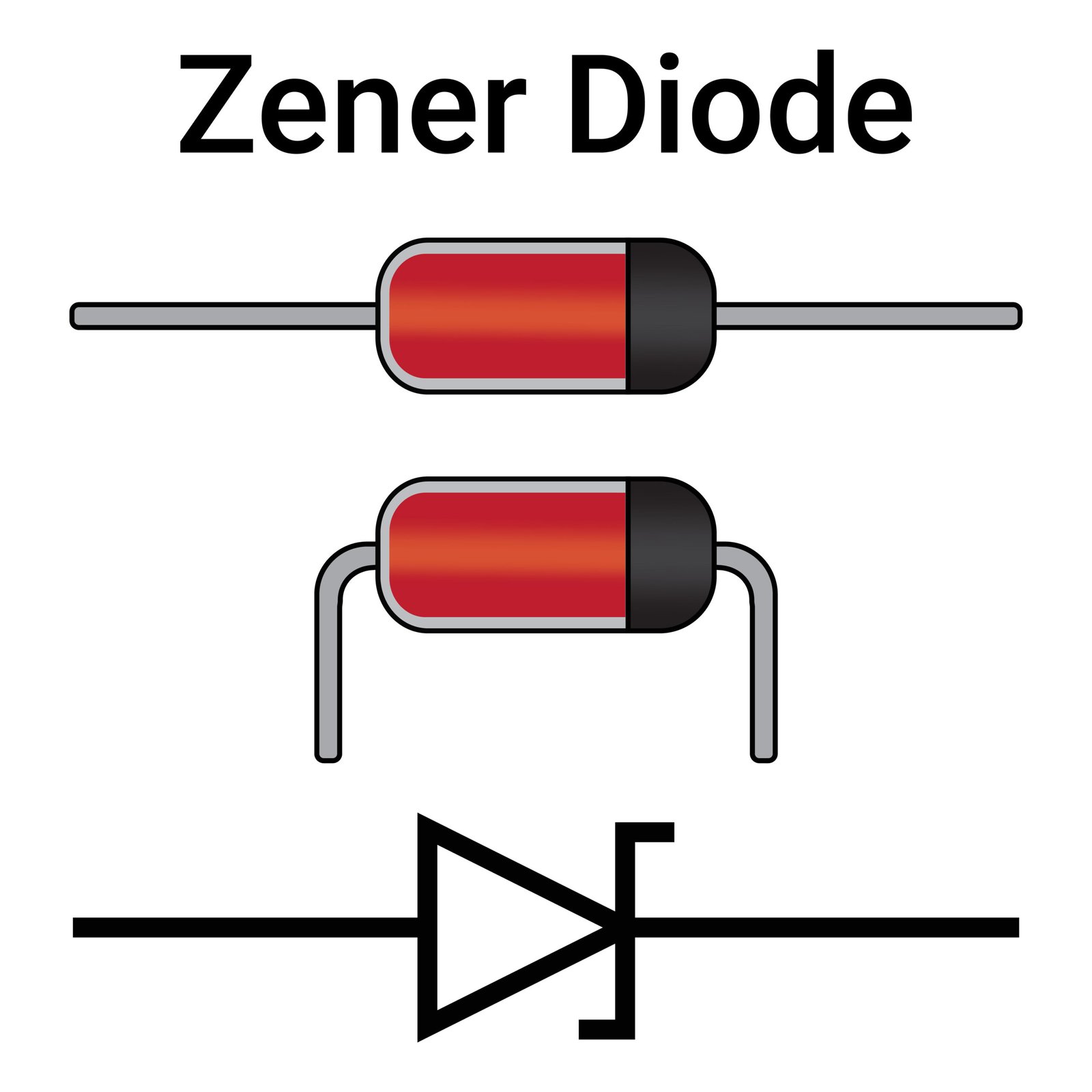
💡 Concept: Special diode designed to operate in reverse bias at a fixed Zener voltage.
Below Zener voltage: only leakage current flows.
At Zener breakdown: current increases sharply but voltage remains nearly constant.
✔️ Used as a voltage regulator in power supplies.
📡 Bipolar Junction Transistor (BJT)
Structure:
Three regions: Emitter (heavily doped), Base (thin & lightly doped), Collector (moderately doped).
Types: npn and pnp.
Working:
➡️ A small base current controls a large collector current.
➡️ Relation: IE = IC + IB.
➡️ Current gain β = IC/IB (20–200 typical).
Applications:
✔️ Amplifier (boosts weak signals).
✔️ Switch (used in digital circuits, ON/OFF).
💡 Concept: This small-base, large-collector current relation is the foundation of modern electronics.
🖥️ Logic Gates
Operate on binary inputs (0,1).
Basic Gates
🔵 AND: Output 1 only if all inputs 1.
🟢 OR: Output 1 if any input 1.
🔴 NOT: Inverts input.
Universal Gates
🟠 NAND and NOR: Any logic circuit can be built using only NAND or NOR.
Truth Tables
✔️ AND Gate
(0,0) → 0
(0,1) → 0
(1,0) → 0
(1,1) → 1
✔️ OR Gate
(0,0) → 0
(0,1) → 1
(1,0) → 1
(1,1) → 1
✔️ NOT Gate
0 → 1
1 → 0
✔️ NAND Gate
(0,0) → 1
(0,1) → 1
(1,0) → 1
(1,1) → 0
✔️ NOR Gate
(0,0) → 1
(0,1) → 0
(1,0) → 0
(1,1) → 0
✏️ Note: NAND and NOR are called universal because they can replicate any gate.
🛠️ Applications in Daily Life
✔️ Microprocessors & memory chips (millions of transistors).
✔️ Solar cells (renewable energy).
✔️ LEDs (displays, lighting).
✔️ Photodiodes (sensors, remotes).
✔️ Amplifiers in communication devices.
✔️ Switching in digital computers & automation.
Summary (~300 words)
🔑 Key Points
🔵 Materials: Conductors, Insulators, Semiconductors.
🟢 Band Theory: Valence band, conduction band, band gap.
🔴 Intrinsic and extrinsic semiconductors.
🟡 Doping: n-type and p-type carriers.
✔️ p–n Junction: Depletion region, barrier potential (~0.3 V Ge, ~0.7 V Si).
✔️ Diodes: Forward bias → conduction, Reverse bias → small constant current.
✔️ Rectifiers: Half-wave and full-wave convert AC to DC.
✔️ Zener diode: Maintains constant voltage in breakdown.
✔️ BJT: Three-terminal device; small base current controls large collector current.
✔️ Logic Gates: AND, OR, NOT, NAND, NOR (with truth tables).
🌿 Importance
Semiconductors are the core of digital technology.
They enabled computers, communication, renewable energy devices.
From household appliances to satellites, they power modern civilization.
📝 Quick Recap
✔️ Semiconductors lie between conductors & insulators.
✔️ Doping → n-type & p-type.
✔️ Barrier potentials: ~0.3 V (Ge), ~0.7 V (Si).
✔️ Diodes → Forward bias conduction, Reverse bias → minority current.
✔️ Rectifiers, LEDs, Zener regulators → Diode applications.
✔️ BJT → Amplifier & Switch.
✔️ Logic Gates (AND, OR, NOT, NAND, NOR) → Digital foundation.
————————————————————————————————————————————————————————————————————————————
QUESTIONS FROM TEXTBOOK
Question 14.1
In an n-type silicon, which of the following statements is true:
🔵 (A) Electrons are majority carriers and trivalent atoms are the dopants.
🟢 (B) Electrons are minority carriers and pentavalent atoms are the dopants.
🟠 (C) Holes are minority carriers and pentavalent atoms are the dopants.
🔴 (D) Holes are majority carriers and trivalent atoms are the dopants.
Answer 14.1
➡️ In n-type semiconductors, doping is done with pentavalent atoms (like P, As, Sb).
➡️ This introduces extra electrons as majority carriers, while holes become minority carriers.
✔️ Correct option: 🟠 (C) Holes are minority carriers and pentavalent atoms are the dopants.
Question 14.2
Which of the statements given in Exercise 14.1 is true for p-type semiconductors?
🔵 (A) Electrons are majority carriers and trivalent atoms are the dopants.
🟢 (B) Electrons are minority carriers and pentavalent atoms are the dopants.
🟠 (C) Holes are minority carriers and pentavalent atoms are the dopants.
🔴 (D) Holes are majority carriers and trivalent atoms are the dopants.
Answer 14.2
➡️ In p-type semiconductors, doping is done with trivalent atoms (like B, Al, In).
➡️ This results in holes as majority carriers, and electrons act as minority carriers.
✔️ Correct option: 🔴 (D) Holes are majority carriers and trivalent atoms are the dopants.
Question 14.3
Carbon, silicon and germanium have four valence electrons each. These are characterised by valence and conduction bands separated by energy band gaps equal to (Eg)C, (Eg)Si and (Eg)Ge. Which of the following statements is true?
🔵 (A) (Eg)Si < (Eg)Ge < (Eg)C 🟢 (B) (Eg)C < (Eg)Ge < (Eg)Si 🟠 (C) (Eg)C > (Eg)Si > (Eg)Ge
🔴 (D) (Eg)C = (Eg)Si = (Eg)Ge
Answer 14.3
➡️ Band gap values:
Carbon (diamond): ≈ 5.5 eV
Silicon: ≈ 1.1 eV
Germanium: ≈ 0.7 eV
Thus, order: (Eg)C > (Eg)Si > (Eg)Ge.
✔️ Correct option: 🟠 (C) (Eg)C > (Eg)Si > (Eg)Ge.
Question 14.4
In an unbiased p–n junction, holes diffuse from the p-region to n-region because:
🔵 (A) Free electrons in the n-region attract them.
🟢 (B) They move across the junction by the potential difference.
🟠 (C) Hole concentration in p-region is more as compared to n-region.
🔴 (D) All the above.
Answer 14.4
➡️ The diffusion of holes is driven by multiple factors:
Concentration gradient (more holes in p-region than in n-region).
Attraction by electrons in n-region.
Effect of the built-in potential difference.
✔️ Correct option: 🔴 (D) All the above.
Question 14.5
When a forward bias is applied to a p–n junction, it:
🔵 (A) Raises the potential barrier.
🟢 (B) Reduces the majority carrier current to zero.
🟠 (C) Lowers the potential barrier.
🔴 (D) None of the above.
Answer 14.5
➡️ Applying forward bias decreases the depletion width.
➡️ This lowers the potential barrier, allowing majority carriers to cross the junction easily.
✔️ Correct option: 🟠 (C) Lowers the potential barrier.
Question 14.6
In half-wave rectification, what is the output frequency if the input frequency is 50 Hz? What is the output frequency of a full-wave rectifier for the same input frequency?
Answer 14.6
➡️ Half-wave rectifier:
Only one half cycle of AC is used.
Output frequency = Input frequency = 50 Hz.
➡️ Full-wave rectifier:
Both half cycles contribute.
Output frequency = 2 × Input frequency = 100 Hz.
Final Answer:
Half-wave rectifier output frequency = 50 Hz
Full-wave rectifier output frequency = 100 Hz
————————————————————————————————————————————————————————————————————————————
OTHER IMPORTANT QUESTIONS
(CBSE MODEL QUESTIONS PAPER)
ESPECIALLY MADE FROM THIS LESSON ONLY
Q1. Which of the following has the largest band gap?
🔵 (A) Germanium
🟢 (B) Silicon
🟠 (C) Carbon (diamond)
🔴 (D) Gallium
Answer: 🟠 (C) Carbon (diamond)
Q2. In an n-type semiconductor, the majority carriers are:
🔵 (A) Holes
🟢 (B) Electrons
🟠 (C) Protons
🔴 (D) None
Answer: 🟢 (B) Electrons
Q3. Barrier potential of a Si diode at room temperature is approximately:
🔵 (A) 0.3 V
🟢 (B) 0.5 V
🟠 (C) 0.7 V
🔴 (D) 1.1 V
Answer: 🟠 (C) 0.7 V
Q4. A p-type semiconductor is formed by doping with:
🔵 (A) Pentavalent atom
🟢 (B) Trivalent atom
🟠 (C) Tetravalent atom
🔴 (D) Hexavalent atom
Answer: 🟢 (B) Trivalent atom
Q5. Which diode is used as a voltage regulator?
🔵 (A) Photodiode
🟢 (B) LED
🟠 (C) Zener diode
🔴 (D) Tunnel diode
Answer: 🟠 (C) Zener diode
Q6. The output frequency of a full-wave rectifier for input 50 Hz is:
🔵 (A) 25 Hz
🟢 (B) 50 Hz
🟠 (C) 100 Hz
🔴 (D) 200 Hz
Answer: 🟠 (C) 100 Hz
Q7. In forward bias, the width of depletion layer:
🔵 (A) Increases
🟢 (B) Decreases
🟠 (C) Becomes zero
🔴 (D) Remains unchanged
Answer: 🟢 (B) Decreases
Q8. In reverse bias, current is mainly due to:
🔵 (A) Majority carriers
🟢 (B) Minority carriers
🟠 (C) Protons
🔴 (D) Holes
Answer: 🟢 (B) Minority carriers
Q9. The energy band gap of Si is:
🔵 (A) 0.3 eV
🟢 (B) 0.7 eV
🟠 (C) 1.1 eV
🔴 (D) 5.5 eV
Answer: 🟠 (C) 1.1 eV
Q10. Which is the universal gate?
🔵 (A) AND
🟢 (B) OR
🟠 (C) NAND
🔴 (D) NOT
Answer: 🟠 (C) NAND
Q11. Which device converts sunlight directly into electricity?
🔵 (A) Photodiode
🟢 (B) LED
🟠 (C) Solar cell
🔴 (D) Zener diode
Answer: 🟠 (C) Solar cell
Q12. The emitter of a transistor is:
🔵 (A) Lightly doped
🟢 (B) Moderately doped
🟠 (C) Heavily doped
🔴 (D) Undoped
Answer: 🟠 (C) Heavily doped
Q13. In logic gates, binary input “0” means:
🔵 (A) High voltage
🟢 (B) Low voltage
🟠 (C) Infinite resistance
🔴 (D) Open circuit
Answer: 🟢 (B) Low voltage
Q14. In common emitter configuration, the output is taken from:
🔵 (A) Collector–Base
🟢 (B) Emitter–Base
🟠 (C) Collector–Emitter
🔴 (D) None
Answer: 🟠 (C) Collector–Emitter
Q15. Which gate gives output “0” only when all inputs are “1”?
🔵 (A) AND
🟢 (B) OR
🟠 (C) NAND
🔴 (D) NOR
Answer: 🟠 (C) NAND
➡️ Explanation: AND gives “1” when all inputs = 1, but NAND gives the inverse → output “0” only when all inputs = 1.
Q16. In an npn transistor, majority carriers in emitter are:
🔵 (A) Holes
🟢 (B) Electrons
🟠 (C) Protons
🔴 (D) Neutrons
Answer: 🟢 (B) Electrons
Q17. Which region of a transistor is thin and lightly doped?
🔵 (A) Emitter
🟢 (B) Base
🟠 (C) Collector
🔴 (D) None
Answer: 🟢 (B) Base
Q18. The Boolean expression for OR gate is:
🔵 (A) A • B
🟢 (B) A + B
🟠 (C) A′
🔴 (D) AB′
Answer: 🟢 (B) A + B
Section B (Q19–Q23: Short Answers)
Q19. Why does conductivity of a semiconductor increase with temperature?
Answer: More valence electrons get excited across band gap, creating electron–hole pairs, so conductivity increases.
Q20. Advantage of full-wave rectifier over half-wave rectifier.
Answer: Utilizes both half cycles of AC, higher efficiency (~80%), smoother DC output.
Q21. What happens to depletion width in reverse bias?
Answer: Depletion region widens as potential barrier increases.
Q22. Function of base region in transistor.
Answer: Base is thin and lightly doped → allows carriers from emitter to reach collector, controls current with small IB.
Q23. Name the gate inverse of AND.
Answer: NAND.
Section C (Q24–Q28: Mid-length)
Q24. Explain I–V characteristics of diode.
Answer:
➡️ Forward bias: negligible current until threshold (0.3 V Ge, 0.7 V Si), then exponential rise.
➡️ Reverse bias: tiny reverse saturation current (minority carriers), sharp increase after breakdown.
Q25. Input 60 Hz to half-wave rectifier. What is output frequency of full-wave rectifier?
Answer: f_out = 2 × 60 Hz = 120 Hz.
Q26. Explain Zener diode as voltage regulator.
Answer: In reverse bias at Zener voltage Vz, current increases sharply but voltage across Zener remains nearly constant → output voltage stable even if input/load changes.
Q27. Transistor has IC = 4.9 mA, IB = 0.1 mA. Find β.
Answer: β = IC / IB = 4.9 / 0.1 = 49.
Q28. Write truth table for NOR gate.
Answer:
(0,0) → 1
(0,1) → 0
(1,0) → 0
(1,1) → 0
Section D (Q29–Q31: Long Answers)
Q29. Explain construction and working of solar cell.
Answer:
➡️ Construction: Thin p–n junction on semiconductor, transparent cover, metal contacts.
➡️ Working: Sunlight photons create e–h pairs; junction field separates them; emf produced; connected load gives current.
Q30. Explain transistor as amplifier.
Answer:
➡️ In CE mode, input is applied at base–emitter, output at collector–emitter.
➡️ Small IB change → large IC change (IC = βIB).
➡️ Output signal is amplified version of input.
Q31. Explain working of full-wave rectifier.
Answer:
➡️ Center-tap or bridge circuit: diodes conduct alternately.
➡️ Both half cycles pass through load in same direction.
➡️ Output: pulsating DC of frequency 2f.
Section E (Q32–Q33: Case/Application)
Q32. A silicon diode is forward biased. Barrier potential = 0.7 V. If input rises from 0 to 1 V, explain diode current.
Answer:
➡️ For V < 0.7 V → negligible current.
➡️ After 0.7 V → current rises exponentially up to 1 V.
Q33. In transistor amplifier, Vin = 10 mV, Vout = 2 V. Find voltage gain.
Answer:
Av = Vout / Vin = 2 / 0.01 = 200.
————————————————————————————————————————————————————————————————————————————
NEET QUESTIONS FROM THIS LESSON
Question 1: In a PN junction diode, the barrier potential is due to
🔵 (A) majority charge carriers
🟢 (B) minority charge carriers
🟠 (C) ions on both sides of junction
🔴 (D) drift current only
Answer: (C) ions on both sides of junction
Year: 2025
Question 2: In a forward-biased PN junction diode, current is due to
🔵 (A) diffusion of majority carriers
🟢 (B) drift of minority carriers
🟠 (C) both diffusion and drift
🔴 (D) barrier breakdown
Answer: (A) diffusion of majority carriers
Year: 2025
Question 3: Which type of semiconductor is formed when silicon is doped with phosphorus?
🔵 (A) P-type
🟢 (B) N-type
🟠 (C) Intrinsic
🔴 (D) None
Answer: (B) N-type
Year: 2025
Question 4: In a full-wave rectifier using two diodes, the output frequency is
🔵 (A) equal to input frequency
🟢 (B) half of input frequency
🟠 (C) double of input frequency
🔴 (D) zero
Answer: (C) double of input frequency
Year: 2024
Question 5: In an n-type semiconductor, the majority carriers are
🔵 (A) holes
🟢 (B) electrons
🟠 (C) both
🔴 (D) none
Answer: (B) electrons
Year: 2024
Question 6: The forbidden energy gap in silicon is
🔵 (A) 0.7 eV
🟢 (B) 1.1 eV
🟠 (C) 3.0 eV
🔴 (D) 5.5 eV
Answer: (B) 1.1 eV
Year: 2024
Question 7: The function of a rectifier is to
🔵 (A) convert AC into DC
🟢 (B) convert DC into AC
🟠 (C) increase AC voltage
🔴 (D) decrease AC voltage
Answer: (A) convert AC into DC
Year: 2024
Question 8: In a transistor, the input is always applied between
🔵 (A) base and collector
🟢 (B) base and emitter
🟠 (C) emitter and collector
🔴 (D) collector and ground
Answer: (B) base and emitter
Year: 2024
Question 9: The output characteristics of a transistor in common-emitter configuration is a plot between
🔵 (A) IC and VCE
🟢 (B) IB and VBE
🟠 (C) IC and IB
🔴 (D) VCE and VBE
Answer: (A) IC and VCE
Year: 2023
Question 10: In a common-emitter amplifier, the phase difference between input and output signals is
🔵 (A) 0°
🟢 (B) 90°
🟠 (C) 180°
🔴 (D) 360°
Answer: (C) 180°
Year: 2023
Question 11: Which logic gate has output 1 when both inputs are 0?
🔵 (A) AND
🟢 (B) OR
🟠 (C) NOR
🔴 (D) NAND
Answer: (C) NOR
Year: 2023
Question 12: Which of the following is not a semiconductor?
🔵 (A) Silicon
🟢 (B) Germanium
🟠 (C) Copper
🔴 (D) Gallium arsenide
Answer: (C) Copper
Year: 2023
Question 13: The majority carriers in p-type semiconductor are
🔵 (A) electrons
🟢 (B) holes
🟠 (C) protons
🔴 (D) both electrons and holes equally
Answer: (B) holes
Year: 2022
Question 14: The Boolean expression A·B + A·B̅ is equivalent to
🔵 (A) A
🟢 (B) B
🟠 (C) A + B
🔴 (D) AB
Answer: (A) A
Year: 2022
Question 15: The common-base current gain α is related to common-emitter current gain β as
🔵 (A) α = β/(1 + β)
🟢 (B) β = α/(1 − α)
🟠 (C) both
🔴 (D) none
Answer: (C) both
Year: 2022
Question 16: In a half-wave rectifier, the ratio of RMS value to average value of current is approximately
🔵 (A) 1.11
🟢 (B) 1.21
🟠 (C) 1.57
🔴 (D) 0.45
Answer: (A) 1.11
Year: 2022
Question 17: The logic gate which is called universal gate is
🔵 (A) OR
🟢 (B) AND
🟠 (C) NAND
🔴 (D) NOR
Answer: (C) NAND
Year: 2021
Question 18: The energy gap of an insulator is typically
🔵 (A) <1 eV 🟢 (B) ~1 eV 🟠 (C) 1–3 eV 🔴 (D) >5 eV
Answer: (D) >5 eV
Year: 2021
Question 19: The transfer characteristic of a transistor relates
🔵 (A) IC vs VCE
🟢 (B) IC vs IB
🟠 (C) IC vs VBE
🔴 (D) IC vs IE
Answer: (C) IC vs VBE
Year: 2021
Question 20: The output of a NAND gate is 0 when
🔵 (A) both inputs are 0
🟢 (B) both inputs are 1
🟠 (C) one input is 1
🔴 (D) one input is 0
Answer: (B) both inputs are 1
Year: 2020
Question 21: In a PN junction diode under reverse bias, current is due to
🔵 (A) majority carriers
🟢 (B) minority carriers
🟠 (C) both
🔴 (D) ions
Answer: (B) minority carriers
Year: 2020
Question 22: The output of an OR gate is 1 when
🔵 (A) both inputs are 0
🟢 (B) both inputs are 1
🟠 (C) at least one input is 1
🔴 (D) none
Answer: (C) at least one input is 1
Year: 2020
Question 23: Which material is used in making LED?
🔵 (A) Si
🟢 (B) Ge
🟠 (C) GaAs
🔴 (D) Cu
Answer: (C) GaAs
Year: 2020
Question 24: In an intrinsic semiconductor, the number of electrons is equal to
🔵 (A) number of holes
🟢 (B) zero
🟠 (C) number of protons
🔴 (D) none
Answer: (A) number of holes
Year: 2019
Question 25: The function of Zener diode is
🔵 (A) amplification
🟢 (B) rectification
🟠 (C) voltage regulation
🔴 (D) oscillation
Answer: (C) voltage regulation
Year: 2019
Question 26: The input resistance of a transistor in common-emitter mode is of the order of
🔵 (A) a few ohms
🟢 (B) a few hundred ohms
🟠 (C) a few kilo-ohms
🔴 (D) a few mega-ohms
Answer: (B) a few hundred ohms
Year: 2019
Question 27: The output of an AND gate is 1 when
🔵 (A) both inputs are 1
🟢 (B) both inputs are 0
🟠 (C) any one input is 1
🔴 (D) none
Answer: (A) both inputs are 1
Year: 2019
Question 28: A transistor acts as a switch when it is in
🔵 (A) active region
🟢 (B) cut-off or saturation region
🟠 (C) forward bias only
🔴 (D) reverse bias only
Answer: (B) cut-off or saturation region
Year: 2018
Question 29: In an NPN transistor, the arrow on emitter shows
🔵 (A) direction of conventional current
🟢 (B) direction of electron current
🟠 (C) direction of hole flow
🔴 (D) direction of applied voltage
Answer: (A) direction of conventional current
Year: 2018
Question 30: The current gain in common-emitter mode is denoted by
🔵 (A) α
🟢 (B) β
🟠 (C) γ
🔴 (D) δ
Answer: (B) β
Year: 2018
Question 31: The NOT gate has
🔵 (A) one input, one output
🟢 (B) two inputs, one output
🟠 (C) one input, two outputs
🔴 (D) two inputs, two outputs
Answer: (A) one input, one output
Year: 2017
Question 32: The band gap of germanium is about
🔵 (A) 0.7 eV
🟢 (B) 1.1 eV
🟠 (C) 3.0 eV
🔴 (D) 5.5 eV
Answer: (A) 0.7 eV
Year: 2017
Question 33: In forward biasing of a PN junction diode
🔵 (A) width of depletion region decreases
🟢 (B) width of depletion region increases
🟠 (C) barrier potential increases
🔴 (D) no current flows
Answer: (A) width of depletion region decreases
Year: 2017
Question 34: The most commonly used semiconductor material is
🔵 (A) Copper
🟢 (B) Silicon
🟠 (C) Aluminium
🔴 (D) Iron
Answer: (B) Silicon
Year: 2016
Question 35: In common-base configuration, the current gain α is always
🔵 (A) <1 🟢 (B) >1
🟠 (C) =1
🔴 (D) zero
Answer: (A) <1
Year: 2016
Question 36: The number of valence electrons in a semiconductor atom is
🔵 (A) 2
🟢 (B) 3
🟠 (C) 4
🔴 (D) 5
Answer: (C) 4
Year: 2016
Question 37: The output of OR gate is 0 when
🔵 (A) both inputs are 1
🟢 (B) both inputs are 0
🟠 (C) one input is 1
🔴 (D) at least one input is 1
Answer: (B) both inputs are 0
Year: 2015
Question 38: The base region of a transistor is
🔵 (A) thick and heavily doped
🟢 (B) thin and lightly doped
🟠 (C) thick and lightly doped
🔴 (D) thin and heavily doped
Answer: (B) thin and lightly doped
Year: 2015
Question 39: The current gain of a transistor in common-emitter mode is 49. The current gain in common-base mode will be approximately
🔵 (A) 0.02
🟢 (B) 0.49
🟠 (C) 0.98
🔴 (D) 1.02
Answer: (C) 0.98
Year: 2015
Question 40: The Zener diode is used in
🔵 (A) rectifier
🟢 (B) voltage regulator
🟠 (C) oscillator
🔴 (D) amplifier
Answer: (B) voltage regulator
Year: 2014
Question 41: Which of the following is a universal logic gate?
🔵 (A) OR
🟢 (B) AND
🟠 (C) NOR
🔴 (D) NAND
Answer: (D) NAND
Year: 2014
Question 42: A semiconductor diode is used as
🔵 (A) amplifier
🟢 (B) oscillator
🟠 (C) rectifier
🔴 (D) modulator
Answer: (C) rectifier
Year: 2014
Question 43: In an intrinsic semiconductor at room temperature, the number of free electrons is of the order of
🔵 (A) 10¹⁰/m³
🟢 (B) 10¹⁶/m³
🟠 (C) 10²²/m³
🔴 (D) 10²⁸/m³
Answer: (B) 10¹⁶/m³
Year: 2013
Question 44: In a PNP transistor, the majority carriers are
🔵 (A) electrons
🟢 (B) holes
🟠 (C) protons
🔴 (D) none
Answer: (B) holes
Year: 2013
Question 45: Which logic gate is represented by the Boolean expression (A + B)’?
🔵 (A) NOR
🟢 (B) NAND
🟠 (C) AND
🔴 (D) OR
Answer: (A) NOR
Year: 2012
Question 46: In a transistor, the emitter is
🔵 (A) heavily doped
🟢 (B) lightly doped
🟠 (C) moderately doped
🔴 (D) undoped
Answer: (A) heavily doped
Year: 2012
Question 47: The current amplification factor β of a transistor is 49. Then α is approximately
🔵 (A) 0.02
🟢 (B) 0.5
🟠 (C) 0.98
🔴 (D) 1.02
Answer: (C) 0.98
Year: 2011
Question 48: The minority carriers in an n-type semiconductor are
🔵 (A) electrons
🟢 (B) holes
🟠 (C) both
🔴 (D) none
Answer: (B) holes
Year: 2011
Question 49: The output of AND gate is 0 when
🔵 (A) both inputs are 1
🟢 (B) one input is 0
🟠 (C) both inputs are 0
🔴 (D) none
Answer: (B) one input is 0
Year: 2010
Question 50: The collector region of a transistor is
🔵 (A) thin and heavily doped
🟢 (B) thick and lightly doped
🟠 (C) thick and heavily doped
🔴 (D) thin and lightly doped
Answer: (B) thick and lightly doped
Year: 2009
————————————————————————————————————————————————————————————————————————————
JEE MAINS QUESTIONS FROM THIS LESSON
Question 1: In a p–n junction diode under forward bias, the current is due to
🔵 (A) drift of carriers
🟢 (B) diffusion of carriers
🟠 (C) thermionic emission
🔴 (D) tunneling
Answer: (B) diffusion of carriers
Year: 2025 | Shift 1
Question 2: The forbidden energy gap in a conductor is
🔵 (A) large
🟢 (B) small
🟠 (C) zero
🔴 (D) infinite
Answer: (C) zero
Year: 2025 | Shift 2
Question 3: In a transistor, the input resistance is
🔵 (A) low
🟢 (B) very high
🟠 (C) zero
🔴 (D) infinite
Answer: (A) low
Year: 2024 | Jan Shift 1
Question 4: A diode is used in a rectifier because
🔵 (A) it has high resistance in both directions
🟢 (B) it has low resistance in both directions
🟠 (C) it conducts only in one direction
🔴 (D) it blocks current in both directions
Answer: (C) it conducts only in one direction
Year: 2024 | Apr Shift 1
Question 5: The energy band gap of silicon at room temperature is about
🔵 (A) 0 eV
🟢 (B) 0.7 eV
🟠 (C) 1.1 eV
🔴 (D) 3.1 eV
Answer: (C) 1.1 eV
Year: 2024 | Jan Shift 2
Question 6: In n-type semiconductor, the majority charge carriers are
🔵 (A) electrons
🟢 (B) holes
🟠 (C) neutrons
🔴 (D) protons
Answer: (A) electrons
Year: 2024 | Apr Shift 2
Question 7: In full-wave rectifier, the ratio of DC value to RMS value is
🔵 (A) 0.45
🟢 (B) 0.5
🟠 (C) 0.9
🔴 (D) 1.0
Answer: (C) 0.9
Year: 2023 | Jan Shift 1
Question 8: The output of NOT gate is
🔵 (A) same as input
🟢 (B) inverse of input
🟠 (C) double of input
🔴 (D) none
Answer: (B) inverse of input
Year: 2023 | Apr Shift 1
Question 9: The common base transistor configuration has
🔵 (A) high input resistance, high output resistance
🟢 (B) low input resistance, high output resistance
🟠 (C) high input resistance, low output resistance
🔴 (D) low input resistance, low output resistance
Answer: (B) low input resistance, high output resistance
Year: 2023 | Apr Shift 2
Question 10: In half-wave rectifier, the efficiency is about
🔵 (A) 40.6%
🟢 (B) 81.2%
🟠 (C) 20.3%
🔴 (D) 100%
Answer: (A) 40.6%
Year: 2022 | Jun Shift 1
Question 11: The potential barrier of silicon diode is about
🔵 (A) 0.3 V
🟢 (B) 0.7 V
🟠 (C) 1.1 V
🔴 (D) 1.5 V
Answer: (B) 0.7 V
Year: 2022 | Jul Shift 1
Question 12: A Zener diode is used for
🔵 (A) amplification
🟢 (B) rectification
🟠 (C) voltage regulation
🔴 (D) oscillation
Answer: (C) voltage regulation
Year: 2022 | Jun Shift 2
Question 13: The Boolean expression Y = A + 0 simplifies to
🔵 (A) A
🟢 (B) 1
🟠 (C) 0
🔴 (D) A’
Answer: (A) A
Year: 2021 | Feb Shift 1
Question 14: In an intrinsic semiconductor, number of electrons and holes are
🔵 (A) unequal
🟢 (B) equal
🟠 (C) infinite
🔴 (D) zero
Answer: (B) equal
Year: 2021 | Mar Shift 1
Question 15: Which logic gate is called the “universal gate”?
🔵 (A) AND
🟢 (B) OR
🟠 (C) NAND
🔴 (D) NOR
Answer: (C) NAND
Year: 2021 | Jul Shift 1
Question 16: In common emitter transistor, the current gain β is
🔵 (A) Ic/Ib
🟢 (B) Ie/Ic
🟠 (C) Ib/Ic
🔴 (D) Ic/Ie
Answer: (A) Ic/Ib
Year: 2021 | Mar Shift 2
Question 17: The ratio of Ic to Ie in a transistor is
🔵 (A) 0.95
🟢 (B) 0.5
🟠 (C) 0.1
🔴 (D) 1.0
Answer: (A) 0.95
Year: 2020 | Jan Shift 1
Question 18: The energy gap of germanium is
🔵 (A) 0.7 eV
🟢 (B) 1.1 eV
🟠 (C) 3.1 eV
🔴 (D) 0 eV
Answer: (A) 0.7 eV
Year: 2020 | Sept Shift 1
Question 19: A photodiode is operated in
🔵 (A) reverse bias
🟢 (B) forward bias
🟠 (C) no bias
🔴 (D) alternating bias
Answer: (A) reverse bias
Year: 2020 | Sept Shift 2
Question 20: The output of AND gate is 1 if
🔵 (A) both inputs are 0
🟢 (B) both inputs are 1
🟠 (C) either input is 1
🔴 (D) none
Answer: (B) both inputs are 1
Year: 2019 | Jan Shift 1
Question 21: The output of OR gate is 0 when
🔵 (A) both inputs are 0
🟢 (B) both inputs are 1
🟠 (C) either input is 1
🔴 (D) none
Answer: (A) both inputs are 0
Year: 2019 | Apr Shift 1
Question 22: In transistor action, the base region is
🔵 (A) thick and heavily doped
🟢 (B) thin and lightly doped
🟠 (C) thick and lightly doped
🔴 (D) thin and heavily doped
Answer: (B) thin and lightly doped
Year: 2019 | Apr Shift 2
Question 23: The function of rectifier is
🔵 (A) convert DC to AC
🟢 (B) convert AC to DC
🟠 (C) amplify signal
🔴 (D) stabilize voltage
Answer: (B) convert AC to DC
Year: 2018
Question 24: The common emitter amplifier has
🔵 (A) low current gain, low voltage gain
🟢 (B) high current gain, high voltage gain
🟠 (C) low current gain, high voltage gain
🔴 (D) high current gain, low voltage gain
Answer: (B) high current gain, high voltage gain
Year: 2018
Question 25: The reverse saturation current in diode depends on
🔵 (A) forward voltage
🟢 (B) temperature
🟠 (C) resistance
🔴 (D) doping concentration
Answer: (B) temperature
Year: 2018
Question 26: The output of NOR gate is 1 when
🔵 (A) both inputs are 1
🟢 (B) both inputs are 0
🟠 (C) one input is 1 and other is 0
🔴 (D) none
Answer: (B) both inputs are 0
Year: 2017
Question 27: The logic gate whose output is 1 if and only if inputs are different is
🔵 (A) XOR
🟢 (B) AND
🟠 (C) OR
🔴 (D) NAND
Answer: (A) XOR
Year: 2017
Question 28: In p-type semiconductor, the majority carriers are
🔵 (A) electrons
🟢 (B) holes
🟠 (C) protons
🔴 (D) neutrons
Answer: (B) holes
Year: 2017
Question 29: A forward biased p–n junction has resistance
🔵 (A) low
🟢 (B) high
🟠 (C) infinite
🔴 (D) zero
Answer: (A) low
Year: 2016
Question 30: The depletion region in a p–n junction is formed due to
🔵 (A) drift of charge carriers
🟢 (B) diffusion of charge carriers
🟠 (C) thermal breakdown
🔴 (D) avalanche effect
Answer: (B) diffusion of charge carriers
Year: 2016
Question 31: The cut-in voltage of germanium diode is approximately
🔵 (A) 0.3 V
🟢 (B) 0.7 V
🟠 (C) 1.1 V
🔴 (D) 1.5 V
Answer: (A) 0.3 V
Year: 2016
Question 32: An amplifier with feedback has gain
🔵 (A) less than without feedback
🟢 (B) greater than without feedback
🟠 (C) infinite
🔴 (D) zero
Answer: (A) less than without feedback
Year: 2015
Question 33: In an n–p–n transistor, the arrow on emitter shows
🔵 (A) direction of electron flow
🟢 (B) direction of hole flow
🟠 (C) conventional current flow
🔴 (D) none
Answer: (C) conventional current flow
Year: 2015
Question 34: In full-wave rectifier, the efficiency is about
🔵 (A) 40.6%
🟢 (B) 50%
🟠 (C) 81.2%
🔴 (D) 100%
Answer: (C) 81.2%
Year: 2015
Question 35: Which gate is represented by the symbol (⊕)?
🔵 (A) XOR
🟢 (B) OR
🟠 (C) AND
🔴 (D) NOR
Answer: (A) XOR
Year: 2014
Question 36: A transistor can be used as
🔵 (A) oscillator
🟢 (B) amplifier
🟠 (C) switch
🔴 (D) all of these
Answer: (D) all of these
Year: 2014
Question 37: Which one of the following is a semiconductor?
🔵 (A) Copper
🟢 (B) Aluminium
🟠 (C) Silicon
🔴 (D) Silver
Answer: (C) Silicon
Year: 2014
Question 38: The maximum efficiency of half-wave rectifier is
🔵 (A) 40.6%
🟢 (B) 81.2%
🟠 (C) 50%
🔴 (D) 100%
Answer: (A) 40.6%
Year: 2013
Question 39: The number of possible input combinations for a 2-input logic gate is
🔵 (A) 2
🟢 (B) 4
🟠 (C) 8
🔴 (D) 16
Answer: (B) 4
Year: 2013
Question 40: Zener breakdown occurs due to
🔵 (A) collision ionization
🟢 (B) high doping concentration
🟠 (C) thermal agitation
🔴 (D) none
Answer: (B) high doping concentration
Year: 2013
Question 41: A transistor amplifier in CE mode provides
🔵 (A) voltage gain only
🟢 (B) current gain only
🟠 (C) both voltage and current gain
🔴 (D) no gain
Answer: (C) both voltage and current gain
Year: 2012 (AIEEE)
Question 42: Logic expression A·(B + C) is equivalent to
🔵 (A) AB + AC
🟢 (B) (A + B)(A + C)
🟠 (C) AB + C
🔴 (D) A + BC
Answer: (A) AB + AC
Year: 2012 (AIEEE)
Question 43: The current amplification factor α and β of a transistor are related as
🔵 (A) β = α/(1−α)
🟢 (B) β = 1/(1−α)
🟠 (C) α = β/(1+β)
🔴 (D) both A and C
Answer: (D) both A and C
Year: 2011 (AIEEE)
Question 44: A NAND gate is equivalent to
🔵 (A) AND + NOT
🟢 (B) OR + NOT
🟠 (C) NOR + NOT
🔴 (D) none
Answer: (A) AND + NOT
Year: 2011 (AIEEE)
Question 45: Which of the following is not a logic gate?
🔵 (A) AND
🟢 (B) OR
🟠 (C) NOR
🔴 (D) RECTIFIER
Answer: (D) RECTIFIER
Year: 2011 (AIEEE)
Question 46: The Boolean identity A + A’B =
🔵 (A) A + B
🟢 (B) AB
🟠 (C) A + B’
🔴 (D) AB’
Answer: (A) A + B
Year: 2010 (AIEEE)
Question 47: Which of the following devices works in reverse bias?
🔵 (A) LED
🟢 (B) Photodiode
🟠 (C) Rectifier diode
🔴 (D) Transistor
Answer: (B) Photodiode
Year: 2010 (AIEEE)
Question 48: The common base transistor has current gain
🔵 (A) less than 1
🟢 (B) greater than 1
🟠 (C) equal to 1
🔴 (D) infinite
Answer: (A) less than 1
Year: 2009 (AIEEE)
Question 49: The OR gate output is 1 if
🔵 (A) both inputs are 0
🟢 (B) one or both inputs are 1
🟠 (C) both inputs are 1 only
🔴 (D) none
Answer: (B) one or both inputs are 1
Year: 2009 (AIEEE)
Question 50: The digital circuit building block is
🔵 (A) rectifier
🟢 (B) logic gate
🟠 (C) amplifier
🔴 (D) oscillator
Answer: (B) logic gate
Year: 2008 (AIEEE)
————————————————————————————————————————————————————————————————————————————
JEE ADVANCED QUESTIONS FROM THIS LESSON
Q1. The electrical conductivity of a semiconductor increases with rise in temperature because
🔵 (A) number of free electrons increases
🟢 (B) mobility of electrons increases
🟠 (C) both A and B
🔴 (D) none
Answer: (A) number of free electrons increases
Year: 2023 | Paper 1
Q2. In an intrinsic semiconductor, at absolute zero temperature it behaves as
🔵 (A) perfect insulator
🟢 (B) conductor
🟠 (C) metal
🔴 (D) superconductor
Answer: (A) perfect insulator
Year: 2023 | Paper 1
Q3. A semiconductor diode is used as
🔵 (A) rectifier
🟢 (B) amplifier
🟠 (C) oscillator
🔴 (D) modulator
Answer: (A) rectifier
Year: 2022 | Paper 1
Q4. The majority carriers in n-type semiconductor are
🔵 (A) holes
🟢 (B) electrons
🟠 (C) protons
🔴 (D) neutrons
Answer: (B) electrons
Year: 2022 | Paper 1
Q5. The energy band gap of a semiconductor is of the order of
🔵 (A) 1 eV
🟢 (B) 10 eV
🟠 (C) 0.01 eV
🔴 (D) 100 eV
Answer: (A) 1 eV
Year: 2021 | Paper 1
Q6. In a p-type semiconductor, majority charge carriers are
🔵 (A) electrons
🟢 (B) holes
🟠 (C) neutrons
🔴 (D) protons
Answer: (B) holes
Year: 2021 | Paper 1
Q7. The barrier potential of a p-n junction depends on
🔵 (A) temperature
🟢 (B) type of semiconductor
🟠 (C) doping level
🔴 (D) all of these
Answer: (D) all of these
Year: 2020 | Paper 1
Q8. The function of a photodiode is to
🔵 (A) convert current into light
🟢 (B) detect light intensity
🟠 (C) emit light
🔴 (D) store charge
Answer: (B) detect light intensity
Year: 2020 | Paper 1
Q9. The output of a NOT gate is
🔵 (A) always 0
🟢 (B) always 1
🟠 (C) complement of input
🔴 (D) equal to input
Answer: (C) complement of input
Year: 2019 | Paper 1
Q10. In a transistor in common emitter configuration, current gain β is
🔵 (A) IC/IB
🟢 (B) IB/IC
🟠 (C) IC/IE
🔴 (D) IE/IC
Answer: (A) IC/IB
Year: 2019 | Paper 1
Q11. The current in forward bias diode circuit is
🔵 (A) very small
🟢 (B) large
🟠 (C) zero
🔴 (D) none
Answer: (B) large
Year: 2018 | Paper 1
Q12. In reverse bias, the current across a diode is due to
🔵 (A) majority carriers
🟢 (B) minority carriers
🟠 (C) both
🔴 (D) none
Answer: (B) minority carriers
Year: 2018 | Paper 1
Q13. A solar cell is basically a
🔵 (A) p-n junction
🟢 (B) transistor
🟠 (C) LED
🔴 (D) photomultiplier
Answer: (A) p-n junction
Year: 2017 | Paper 1
Q14. The truth table of AND gate shows output 1 only if
🔵 (A) one input is 1
🟢 (B) both inputs are 1
🟠 (C) both inputs are 0
🔴 (D) either input is 1
Answer: (B) both inputs are 1
Year: 2017 | Paper 1
Q15. In semiconductors, forbidden energy gap is
🔵 (A) small
🟢 (B) large
🟠 (C) zero
🔴 (D) infinite
Answer: (A) small
Year: 2016 | Paper 1
Q16. A Zener diode is used as
🔵 (A) rectifier
🟢 (B) voltage regulator
🟠 (C) amplifier
🔴 (D) oscillator
Answer: (B) voltage regulator
Year: 2016 | Paper 1
Q17. The minority carriers in a p-type semiconductor are
🔵 (A) holes
🟢 (B) electrons
🟠 (C) protons
🔴 (D) positrons
Answer: (B) electrons
Year: 2015 | Paper 1
Q18. In an n-p-n transistor in active mode, the collector current is mainly due to
🔵 (A) holes
🟢 (B) electrons
🟠 (C) protons
🔴 (D) positrons
Answer: (B) electrons
Year: 2023 | Paper 2
Q19. A NAND gate is equivalent to
🔵 (A) AND + NOT
🟢 (B) OR + NOT
🟠 (C) AND only
🔴 (D) NOR only
Answer: (A) AND + NOT
Year: 2023 | Paper 2
Q20. The input resistance of a common emitter transistor amplifier is of the order of
🔵 (A) a few ohms
🟢 (B) kΩ
🟠 (C) MΩ
🔴 (D) zero
Answer: (B) kΩ
Year: 2022 | Paper 2
Q21. In a logic circuit, the output of XOR gate is 1 when
🔵 (A) both inputs are 0
🟢 (B) both inputs are 1
🟠 (C) inputs are different
🔴 (D) inputs are same
Answer: (C) inputs are different
Year: 2022 | Paper 2
Q22. The dynamic resistance of a p-n junction diode in forward bias is of the order of
🔵 (A) Ω
🟢 (B) kΩ
🟠 (C) MΩ
🔴 (D) none
Answer: (A) Ω
Year: 2021 | Paper 2
Q23. The function of LED is to
🔵 (A) detect light
🟢 (B) emit light
🟠 (C) store charge
🔴 (D) rectify AC
Answer: (B) emit light
Year: 2021 | Paper 2
Q24. Which logic gate is known as universal gate?
🔵 (A) OR
🟢 (B) AND
🟠 (C) NAND
🔴 (D) NOR
Answer: (C) NAND
Year: 2020 | Paper 2
Q25. The reverse saturation current in a diode
🔵 (A) decreases with rise in temperature
🟢 (B) increases with rise in temperature
🟠 (C) independent of temperature
🔴 (D) none
Answer: (B) increases with rise in temperature
Year: 2020 | Paper 2
Q26. The output of OR gate is 0 only when
🔵 (A) both inputs are 1
🟢 (B) both inputs are 0
🟠 (C) inputs are different
🔴 (D) one input is 1
Answer: (B) both inputs are 0
Year: 2019 | Paper 2
Q27. In a full-wave rectifier, the efficiency is about
🔵 (A) 40%
🟢 (B) 81%
🟠 (C) 50%
🔴 (D) 100%
Answer: (B) 81%
Year: 2019 | Paper 2
Q28. The output of NOR gate is 1 when
🔵 (A) both inputs are 0
🟢 (B) both inputs are 1
🟠 (C) one input is 1
🔴 (D) inputs are different
Answer: (A) both inputs are 0
Year: 2018 | Paper 2
Q29. Which diode is used for voltage regulation?
🔵 (A) LED
🟢 (B) Zener diode
🟠 (C) Photodiode
🔴 (D) Tunnel diode
Answer: (B) Zener diode
Year: 2018 | Paper 2
Q30. The current gain in common base configuration is denoted by
🔵 (A) α
🟢 (B) β
🟠 (C) γ
🔴 (D) δ
Answer: (A) α
Year: 2017 | Paper 2
Q31. The transistor action is due to
🔵 (A) majority carriers only
🟢 (B) minority carriers only
🟠 (C) both majority and minority
🔴 (D) protons
Answer: (B) minority carriers only
Year: 2017 | Paper 2
Q32. Which material is commonly used for solar cells?
🔵 (A) Germanium
🟢 (B) Silicon
🟠 (C) Gallium Arsenide
🔴 (D) Copper
Answer: (B) Silicon
Year: 2016 | Paper 2
Q33. The output of NAND gate is 0 when
🔵 (A) both inputs are 0
🟢 (B) both inputs are 1
🟠 (C) inputs are different
🔴 (D) either input is 0
Answer: (B) both inputs are 1
Year: 2016 | Paper 2
Q34. Which device converts light energy into electrical energy?
🔵 (A) LED
🟢 (B) Photodiode
🟠 (C) Solar cell
🔴 (D) Zener diode
Answer: (C) Solar cell
Year: 2015 | Paper 2
————————————————————————————————————————————————————————————————————————————
PRACTICE SETS FROM THIS LESSON
Q1–Q20 (NEET Level: Moderate)
Q1. Which property of semiconductors makes them different from metals?
🔵 (A) Conductivity decreases with temperature
🟢 (B) Conductivity increases with temperature
🟠 (C) Conductivity is independent of temperature
🔴 (D) Always act as insulators
Answer: 🟢 (B) Conductivity increases with temperature
Q2. The band gap of germanium at room temperature is:
🔵 (A) 0.3 eV
🟢 (B) 0.7 eV
🟠 (C) 1.1 eV
🔴 (D) 5.5 eV
Answer: 🟢 (B) 0.7 eV
Q3. In a p-type semiconductor, majority carriers are:
🔵 (A) Electrons
🟢 (B) Protons
🟠 (C) Holes
🔴 (D) None
Answer: 🟠 (C) Holes
Q4. Which device converts optical energy into electrical energy?
🔵 (A) LED
🟢 (B) Photodiode
🟠 (C) Solar cell
🔴 (D) Zener diode
Answer: 🟠 (C) Solar cell
Q5. A forward biased Si diode conducts significantly after:
🔵 (A) 0.2 V
🟢 (B) 0.5 V
🟠 (C) 0.7 V
🔴 (D) 1.1 V
Answer: 🟠 (C) 0.7 V
Q6. A reverse biased diode conducts mainly due to:
🔵 (A) Majority carriers
🟢 (B) Minority carriers
🟠 (C) Protons
🔴 (D) Holes only
Answer: 🟢 (B) Minority carriers
Q7. A Zener diode works in:
🔵 (A) Forward bias below 0.7 V
🟢 (B) Forward bias above 0.7 V
🟠 (C) Reverse bias beyond breakdown voltage
🔴 (D) Both forward and reverse bias equally
Answer: 🟠 (C) Reverse bias beyond breakdown voltage
Q8. Which gate has output = 1 only when all inputs are 1?
🔵 (A) OR
🟢 (B) AND
🟠 (C) NAND
🔴 (D) NOR
Answer: 🟢 (B) AND
Q9. Frequency of output of full-wave rectifier for input 50 Hz is:
🔵 (A) 25 Hz
🟢 (B) 50 Hz
🟠 (C) 100 Hz
🔴 (D) 200 Hz
Answer: 🟠 (C) 100 Hz
Q10. The emitter of a transistor is:
🔵 (A) Thin and lightly doped
🟢 (B) Moderately doped
🟠 (C) Thick and heavily doped
🔴 (D) Undoped
Answer: 🟠 (C) Thick and heavily doped
Q11. Which region of transistor is thin and lightly doped?
🔵 (A) Emitter
🟢 (B) Base
🟠 (C) Collector
🔴 (D) None
Answer: 🟢 (B) Base
Q12. In logic, 0 represents:
🔵 (A) High voltage
🟢 (B) Low voltage
🟠 (C) Infinite resistance
🔴 (D) Always negative potential
Answer: 🟢 (B) Low voltage
Q13. Current gain in CE configuration is defined as:
🔵 (A) IC / IE
🟢 (B) IC / IB
🟠 (C) IE / IB
🔴 (D) IB / IC
Answer: 🟢 (B) IC / IB
Q14. Which device is used as a light source?
🔵 (A) Photodiode
🟢 (B) LED
🟠 (C) Zener diode
🔴 (D) Solar cell
Answer: 🟢 (B) LED
Q15. The energy band gap of Si is closest to:
🔵 (A) 0.3 eV
🟢 (B) 0.7 eV
🟠 (C) 1.1 eV
🔴 (D) 5.5 eV
Answer: 🟠 (C) 1.1 eV
Q16. Which is a universal gate?
🔵 (A) AND
🟢 (B) OR
🟠 (C) NAND
🔴 (D) NOT
Answer: 🟠 (C) NAND
Q17. Solar cells work on principle of:
🔵 (A) Photoelectric emission
🟢 (B) Photovoltaic effect
🟠 (C) Photoconduction
🔴 (D) Thermionic emission
Answer: 🟢 (B) Photovoltaic effect
Q18. The collector of a transistor is:
🔵 (A) Heavily doped
🟢 (B) Lightly doped and larger in size
🟠 (C) Undoped
🔴 (D) Same as emitter
Answer: 🟢 (B) Lightly doped and larger in size
Q19. The output of an OR gate is 0 only when:
🔵 (A) Both inputs are 0
🟢 (B) Both inputs are 1
🟠 (C) Any input is 1
🔴 (D) None
Answer: 🔵 (A) Both inputs are 0
Q20. A NOT gate output is 1 when input is:
🔵 (A) 0
🟢 (B) 1
🟠 (C) Both 0 and 1
🔴 (D) None
Answer: 🔵 (A) 0
Q21–Q40 (JEE Main Level: Enhanced)
Q21. In Si diode, current doubles for every ~10 °C rise in temperature because:
🔵 (A) Resistance decreases
🟢 (B) Minority carriers increase exponentially
🟠 (C) Band gap reduces to zero
🔴 (D) Depletion width vanishes
Answer: 🟢 (B) Minority carriers increase exponentially
Q22. A transistor is used as amplifier in CE mode. If input resistance = 2 kΩ and current gain β = 50, load resistance = 5 kΩ, find voltage gain (Av).
🔵 (A) 50
🟢 (B) 100
🟠 (C) 125
🔴 (D) 250
Answer: 🟠 (C) 125
Q23. The output of NAND gate for inputs (1, 1) is:
🔵 (A) 0
🟢 (B) 1
🟠 (C) Depends on voltage
🔴 (D) Undefined
Answer: 🔵 (A) 0
Q24. The reverse saturation current in a diode is:
🔵 (A) Strongly dependent on applied voltage
🟢 (B) Independent of applied voltage
🟠 (C) Zero at room temp
🔴 (D) Infinite at breakdown
Answer: 🟢 (B) Independent of applied voltage
Q25. The common emitter configuration provides:
🔵 (A) Low input resistance, high output resistance
🟢 (B) High input, low output
🟠 (C) Both high
🔴 (D) Both low
Answer: 🔵 (A) Low input, high output resistance
Q26. A logic gate has output 1 for all inputs 0, and 0 otherwise. It is:
🔵 (A) NOR
🟢 (B) NAND
🟠 (C) OR
🔴 (D) AND
Answer: 🔵 (A) NOR
Q27. For IC = 9 mA and IB = 0.2 mA, β is:
🔵 (A) 25
🟢 (B) 45
🟠 (C) 50
🔴 (D) 90
Answer: 🟠 (C) 50
Q28. A rectifier converts:
🔵 (A) DC to AC
🟢 (B) AC to DC
🟠 (C) High to low voltage
🔴 (D) Low to high voltage
Answer: 🟢 (B) AC to DC
Q29. Which factor controls breakdown voltage of Zener diode?
🔵 (A) Doping concentration
🟢 (B) Temperature only
🟠 (C) Barrier potential only
🔴 (D) Material resistivity
Answer: 🔵 (A) Doping concentration
Q30. In Boolean algebra, A + A′ = ?
🔵 (A) 1
🟢 (B) 0
🟠 (C) A
🔴 (D) A′
Answer: 🔵 (A) 1
Q31. An amplifier has gain = 200. If input = 5 mV, output = ?
🔵 (A) 0.1 V
🟢 (B) 1 V
🟠 (C) 10 V
🔴 (D) 100 V
Answer: 🟠 (C) 10 V
Q32. A solar cell has efficiency 20%. If 100 W sunlight falls, output = ?
🔵 (A) 10 W
🟢 (B) 15 W
🟠 (C) 20 W
🔴 (D) 25 W
Answer: 🟠 (C) 20 W
Q33. In p–n junction, barrier potential depends on:
🔵 (A) Material and temperature
🟢 (B) Only material
🟠 (C) Only doping level
🔴 (D) None
Answer: 🔵 (A) Material and temperature
Q34. The transistor action is due to:
🔵 (A) Majority carriers
🟢 (B) Minority carriers
🟠 (C) Photons
🔴 (D) Holes only
Answer: 🔵 (A) Majority carriers
Q35. The truth table of NOT gate is same as:
🔵 (A) Inverter
🟢 (B) Buffer
🟠 (C) OR
🔴 (D) AND
Answer: 🔵 (A) Inverter
Q36. An input signal of 20 mV is amplified to 2 V. Gain = ?
🔵 (A) 10
🟢 (B) 20
🟠 (C) 100
🔴 (D) 200
Answer: 🔴 (D) 200
Q37. Which logic gate output is 0 when both inputs are 1?
🔵 (A) NAND
🟢 (B) OR
🟠 (C) AND
🔴 (D) NOR
Answer: 🔵 (A) NAND
Q38. A diode in reverse bias behaves like:
🔵 (A) High resistance
🟢 (B) Low resistance
🟠 (C) Zero resistance
🔴 (D) Infinite current source
Answer: 🔵 (A) High resistance
Q39. In a transistor, IC = 4.8 mA, IE = 5 mA. IB = ?
🔵 (A) 0.1 mA
🟢 (B) 0.2 mA
🟠 (C) 0.5 mA
🔴 (D) 1 mA
Answer: 🟢 (B) 0.2 mA
Q40. Which Boolean identity is correct?
🔵 (A) A + AB = A
🟢 (B) A(A + B) = B
🟠 (C) A + 0 = 0
🔴 (D) A · 1 = 0
Answer: 🔵 (A) A + AB = A
Q41–Q50 (JEE Advanced Level: Highest Difficulty)
Q41. A Si diode has barrier 0.7 V. If forward current = 10 mA at 0.7 V, estimate current at 0.8 V (assume exponential, ideal).
🔵 (A) 10 mA
🟢 (B) 20 mA
🟠 (C) ~100 mA
🔴 (D) ~1 A
Answer: 🟠 (C) ~100 mA
Q42. In CE amplifier, if input resistance = 1 kΩ, load = 10 kΩ, β = 100, then voltage gain ≈ ?
🔵 (A) 50
🟢 (B) 100
🟠 (C) 1000
🔴 (D) 10,000
Answer: 🟠 (C) 1000
Q43. If doping concentration in Zener is doubled, breakdown voltage:
🔵 (A) Increases
🟢 (B) Decreases
🟠 (C) Unchanged
🔴 (D) Doubles
Answer: 🟢 (B) Decreases
Q44. A transistor has β = 100, IC = 10 mA. IB = ?
🔵 (A) 10 μA
🟢 (B) 0.1 mA
🟠 (C) 1 mA
🔴 (D) 100 mA
Answer: 🟢 (B) 0.1 mA
Q45. Which configuration has highest voltage gain?
🔵 (A) Common emitter
🟢 (B) Common base
🟠 (C) Common collector
🔴 (D) All equal
Answer: 🔵 (A) Common emitter
Q46. The energy required to move electron from valence to conduction band is called:
🔵 (A) Work function
🟢 (B) Band gap
🟠 (C) Ionization energy
🔴 (D) Fermi energy
Answer: 🟢 (B) Band gap
Q47. If Vin = 20 mV, Vout = 4 V, power gain = ? (Assume same resistance).
🔵 (A) 100
🟢 (B) 200
🟠 (C) 400
🔴 (D) 20,000
Answer: 🟠 (C) 400
Q48. Two NAND gates connected in series give:
🔵 (A) OR
🟢 (B) AND
🟠 (C) NOT
🔴 (D) NOR
Answer: 🟠 (C) NOT
Q49. The dynamic resistance of diode in forward bias decreases because:
🔵 (A) More majority carriers injected
🟢 (B) Barrier widens
🟠 (C) Temperature falls
🔴 (D) Doping reduces
Answer: 🔵 (A) More majority carriers injected
Q50. The maximum efficiency of full-wave rectifier is about:
🔵 (A) 20%
🟢 (B) 40%
🟠 (C) 60%
🔴 (D) 81%
Answer: 🔴 (D) 81%
————————————————————————————————————————————————————————————————————————————
MIND MAP
————————————————————————————————————————————————————————————————————————————